|
|
| |
Keynote Speakers |
|
|
|
|
|
|
|
| |
|

|
|
Daniel Ahmed |
|
Assistant Professor |
|
Acoustics Robotics Systems Lab |
| Institute of Robotics and Intelligent Systems |
| Department of Mechanical and Process Engineering |
|
ETH Zürich, Switzerland |
|
Personal homepage |
|
|
|
Title: Ultrasound-controlled Swarmbots in Physiological Flows |
|
Abstract: Precise, accurate, and controlled motion of microrobots can create new opportunities in targeted and precise delivery of drugs or genes, transducing forces on specific cells or tissues, performing biopsies, and use in non-invasive surgery. However, the application of micro/nanorobots in medicine is fundamentally limited, especially in the vasculature where they need to be manipulated within an imposed blood flow. Typically, tiny agents follow the bloodstream of the vasculature with little to no control in the circulatory system. The ability to propel against the flow or undergo upstream motility would help micro/nanoparticles navigate to a specific site, which could lead to a paradigm shift in targeted drug delivery in medicine. In this talk, I will present swarm-based microrobots in a combination of acoustic and magnetic fields and then purely in ultrasound that shows upstream and cross-stream motion under physiological relevant flows. |
|
|
|

|
|
Andrea Alù |
|
Director, Photonics Initiative |
|
Einstein Professor of Physics |
| Professor of Electrical Engineering |
| Advanced Science Research Center |
|
The City College of New York, USA |
|
Personal homepage |
|
|
|
Title: Metamaterials Baked on Broken Symmetries |
|
Abstract: In this talk, I discuss our recent research activity in electromagnetics, nano-optics, acoustics and mechanics, showing how suitably engineered materials at the nanoscale forming metamaterials open exciting venues to realize new phenomena and devices for light, radio-waves and sound. I discuss venues to induce emerging phenomena stemming from broken geometrical symmetries, to largely break Lorentz reciprocity and realize isolation without the need of magnetic bias based on broken time-reversal symmetry induced by mechanical motion, spatio-temporal modulation and/or nonlinearities. I also discuss how broken symmetries in space and space-time can open the opportunity to induce topological order in metamaterials. Another class of interesting metamaterials based on broken symmetries are parity-time symmetric metamaterials, which are asymmetric in space, but symmetric upon parity and time inversion. In the talk, I will also discuss the impact of these concepts from basic science to practical technology, from classical waves to quantum phenomena. |
|
|
|

|
|
Tatsuo Arai |
|
Professor |
|
Beijing Advanced Innovation Center for Intelligent Robots and Systems |
| Beijing Institute of Technology, China |
|
Visiting Professor of Global Alliance Laboratory |
|
University of Electro-Communication, Japan |
|
Personal homepage |
|
|
|
Title: Micro Robotics Advances Bio Sciences |
|
Abstract: We have been working on micro robotics including dexterous high-speed micromanipulation, micro assembly, cell characterization, and 3D cellular system construction. The basic idea is to devise and to utilize dexterous two finger micro hands, and to achieve total micromanipulation system with high-speed vision and interfaces for bio applications. Our system is multi-scalable and can manipulate micro object with the size ranging from one to hundreds micron meters seamlessly. Our constant system improvements and refinements have achieved wide range of workspace with real time 3D information, simple finger setting-up procedure, fine force sensing capability as well as automated calibration, automated picking-and-placing, etc. Based on these activities and our collaboration experiences with biologists and medical doctors we carried out 5-year national project on “Bio Assembler” in 2011-2016, whose target is a challenge of constructing artificial 3D cellular system in vitro. The major topics are high-speed cell characterization & sorting, 3D cellular system construction, and cell functionalization analysis. Now we are looking at more advanced researches and developments in new bio application fields, such as causality of various stresses in differentiation, proliferation, generation, development, and disease. The mechano biology is one of the examples of such activities and currently so active in biology and medical, however, we are looking for more than that, not just limited to the mechanical matter. We will try to collect as many precise physiological data as possible corresponding to various multi-modal stresses and to clarify novel biological findings by applying the system science principles. |
|
|
|

|
|
Emmanuel Brousseau |
|
Assistant Professor |
|
High Value Manufacturing Research Group |
| Department of Mechanical Engineering |
|
School of Engineering |
|
Cardiff University, United Kingdom |
|
Personal homepage |
|
|
|
Title: Machining with the tip of an AFM probe: research efforts towards an alternative nano-manufacturing process |
|
Abstract: The controlled nano-scale removal of material from the surface of a workpiece conducted with the tip of an Atomic Force Microscope (AFM) probe is a technique which has gained increased attention in the past decade within the micro- and nano-manufacturing research community. The attractive characteristics of this process are that it is relatively simple to implement and it is low-cost compared with vacuum-based lithography techniques for micro- and nano-fabrication. This presentation will provide an overview of a number of research investigations conducted at Cardiff University (UK) in the field of AFM probe-based machining in the past 10 years. The reported work will include a range of experimental and theoretical studies and will also cover recent results from a specific application of the process in the field of nano-magnetism. |
|
|
|

|
|
Feng Chen |
|
Professor, Director |
|
Ultrafast Photonic Laboratory (UPL) |
|
Director of Shaanxi Key Laboratory of Photonics Technology for Information (PTI) |
| Xi'an Jiaotong University |
|
Xi'an, China |
|
Personal homepage |
|
|
|
Title: Femtosecond laser bionic fabrication |
|
Abstract: Biological micro/nano-structures all comprise the goals for the next-generation smart artificial materials and devices. This presentation summarizes the recent progress in the development of bioinspired smart structures via femtosecond laser micro/nanofabrication, with a focus on controllable, biomimetic, and switchable wetting surfaces, as well as their applications in biology, micro-optics, and industry, all of which demonstrate the ability of laser microfabrication in producing various multiscale structures and its adaptation in a great variety of materials. The current challenges and future research prospects of this rapidly developing field are also being discussed. |
|
|
|

|
|
Harald Fuchs |
|
Professor |
|
Head |
| Physikalisches Institut and Center for Nanotechnology (CeNTech) |
| Westfälische Wilhelms-Universität Münster |
|
Germany |
|
Personal homepage |
|
|
|
Title: From chemical bonds to molecular assemblers |
|
Abstract: Surfaces and interfaces represent low-dimensional spatial confinements opening unique pathways towards on-surface chemical reaction schemes with regio-selective and kinetic control that is not available in conventional liquid- or gas-phase chemistry. In addition, surfaces may be catalytically active, and by surface reconstruction or faceting the spatial confinement may display one- or zero-dimensional character. Beyond pure mechanical support, surfaces may also promote ordering by self-assembly of educts and products and may stabilize them by molecule-substrate interactions. We have studied numerous novel chemical surface reaction types including metal-organic compounds, precursors for generating graphdiynes, and peroxides, otherwise unstable in liquid or gas phases [1]. By using on-surface chemistry techniques intermediate states can be analyzed with high resolution techniques such as low-temperature STM and AFM under ultrahigh vacuum condition. This approach also opens the pathway for controlled orthogonal reactions. Beyond all that, we found a fascinating new and powerful potential of on-surface chemistry which allows to set up a new strategy for the generation of intelligent functional systems. In this context, we recently introduced a molecular swarm like system performing a coordinated surface restructuring. It is based on N‐heterocyclic carbenes (NHC) binding to a single noble metal atom such as of an Au(111) surface after vacuum deposition. Depending on the type of N-ligands, NHCs are able to pull a single atom out of the surface after forming a covalent bond and then travel in the so-called ‘ballbot’- motion type across the surface, eventually forming densely packed islands [2]. The ballbots form spontaneously on the surface. We discovered that on an Au(1x2) reconstructed surface ballbot-NHcs are able to autonomously re-organize that surface atom by atom in a well-controlled and ‘swarm-like’ manor [3]. No external supporting measures are required such as lithography or STM and AFM probes. Rather, the cooperative restructuring occurs in a special zipper-mode by the molecular machines which are re-arranging Au atoms with atomic precision and in a massive parallel scheme. As a result, the Au(1x2) surface is transferred at room temperature into an Au(1x3) -‘Added Row (AR)’ structure. It is known that the Au(1x3)-AR surface displays a higher chemical reactivity than the native Au(1x2) structure and does not spontaneously transform back to the (1x2) reconstruction as does the conventional Au(1x3) reconstruction occurring at temperatures around 800 K on a clean Au (111) surface. This observation opens the door for the generation of ‘programmed’ and autonomously acting molecular species possibly allowing to optimize surfaces in a cooperative way, for example, for catalysis applications.
|
|
|
|

|
|
Ambarish Ghosh |
|
Associate Professor |
|
Center for Nano Science and Engineering |
|
Indian Institute of Science |
| Bangalore |
|
India |
|
Personal homepage |
|
|
|
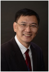
Title: Multifunctional helical nanobots: roles of material and geometry |
|
Abstract: Helical nanobots driven by magnetic fields can provide mechanical information about their local surrounding with sub-micron spatial resolution, probe complex, heterogenous biological environments, such as the intracellular environment, as well as the extracellular matrix; and provide a rich and powerful platform towards futuristic drug delivery. The same system can be used for sub-micron colloidal cargo manipulation in microfluidic devices and on-chip assembly applications. Their fabrication is based on shadow evaporation allowing a wafer scale route towards integration of many different functionalities in a single nanostructure. Crucially, their properties and functionalities can be tuned with great control using intelligent design of material and geometry, and I will present few examples of the same. |
|
|
|
|
|
Minghui Hong |
|
Professor |
|
Fellow of Optical Society of America |
| Department of Electrical and Computer Engineering |
| National University of Singapore |
|
Singapore |
|
Personal homepage |
|
|
|
Title: Laser Precision Engineering: from Micro-scale to Nano-scale |
|
Abstract: Laser precision engineering in ambient air has unique advantages as a non-contact and high-speed process. It is a key advanced manufacturing approach for high quality micro/nano-structures’ fabrication. In the past decades, we have witnessed its extensive applications in research laboratories and production lines. Combined with some advanced processing tools, such as AFM and NSOM, laser precision engineering’s resolution can be pushed down to 10 ~ 25 nm, much smaller than Optical Diffraction Limit, which provides an excellent opportunity for the nano-manufacturing. In this talk, the physics behind laser-matter interactions will be reviewed. How to achieve small heat affected zone (HAZ) is one critical challenge for high quality laser precision engineering to push its resolution from micro-scale to nano-scale. The next critical challenge is how to ensure high enough nano-fabrication speed to meet industrial needs. Since one beam laser processing at high resolution could not achieve such mission, parallel laser beam processing is developed to cater for both high resolution and high speed at the same time. Another challenge is how to carry out the laser nano-structuring in far field as the near field processing requires the tiny optics working very close to sample surfaces, which makes the laser nanofabrication in near field be only suitable for very limited super-smooth surface samples. Our recent research shows that hybrid pulsed laser processing in far field and in ambient air is a novel method to make ~15 nm features directly on Si surfaces. With better understanding of the complicated physics behind this unique experimental result, as well as further fine tuning of our experimental setup and laser processing parameters, it is highly possible to bring our laser precision engineering resolution down to ~10 nm. |
|
|
|

|
|
Ali K. Hoshiar |
|
Assistant professor |
|
School of Computer Science and Electronic Engineering (CSEE) |
| University of Essex |
| UK |
|
|
|
Personal homepage |
|
|
|
Title: Microrobotic systems for swarm delivery of the therapeutics agents |
|
Abstract: The rapid advancement in microrobotic systems in recent years for the medical applications, as well as human scale microrobotics systems, and advancements in the medical monitoring systems (magnetic particle imaging (MPI), fast MRI, and X-ray) lead to the precise control of microswarms in therapeutic delivery applications. However, predicting the nonlinear complex behaviour of the microswarms in the magnetic field remained as an open challenge. In this talk I will present the recent monitoring schemes (e. g. MPI), the practical actuation schemes, and most recent predictive models for microswarm control. |
|
|
|

|
|
Veronica Iacovacci |
|
Marie Curie Fellow |
|
The BioRobotics Institute |
| Scuola Superiore Sant’Anna, Pisa |
| Italy |
|
|
|
Personal homepage |
|
|
|
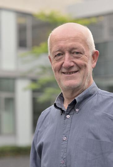
Title: Micro- and nanorobots in the body: monitoring and safety challenges |
|
Abstract: Medical micro- and nanorobots have been demonstrated for a variety of non-invasive biomedical applications, such as tissue engineering, drug delivery, and assisted fertilization, among others. However, most of these demonstrations have been carried out in in vitro settings and under optical microscopy, being significantly different from the clinical practice. Furthermore, the predominant use of magnetic micro and nanostructures might pose force scaling, safety and biodistribution challenges. In this framework, despite astonishing advancements in the fabrication, powering, and control of tiny motile devices, many challenges still prevent micro- and nanorobots route to the clinic.
In this talk, some of these challenges will be analyzed, with a particular focus on how tracking tiny machines in real tissues and how retrieving them upon task execution. |
|
|
|
|
|
Eberhard Manske |
|
Professor |
|
Institute of Process Measurement and Sensor Technology |
| Faculty of Mechanical Engineering |
| Ilmenau University of Technology |
|
Germany |
|
Personal homepage |
|
|
|
Title: Tip- and laser- based nanofabrication in extended areas with sub-nanometre precision |
|
Abstract: For several years, new tip‐based or laser‐based patterning techniques have been attracting increasing attention as alternative lithography approaches. Most tip‐based techniques are based on the use of commercial or modified atomic force microscopes (AFM) and have so far only been demonstrated at the micrometer scale. Direct laser writing is mostly based on galvanoscanners or (similar to the AFM methods) on piezo drives. The biggest disadvantage in all cases, however, is the insufficient measurement and positioning technology.
At the TU Ilmenau, nanopositioning and nanometrology machines based on advanced laser interferometers have been successfully developed over many years, which are able to overcome this deficit. Consequently, this technique is therefore applied to processes of tip‐ and laser‐based manufacturing. This will enable measurement and patterning at the atomic level on both flat and non‐flat surfaces (e.g. precision optical surfaces).
The laser interferometer‐based high‐precision machines now have resolution up to 5 picometers and sub‐nanometer reproducibility in measurement ranges up to 200 mm x 200 mm. They can be used with AFM heads for both lithography purposes and high‐resolution measurement of fabricated structures. In addition, direct laser writing was demonstrated with both single‐photon processes (at 405 nm) and two‐photon processes based on femtosecond lasers. New effects for laser‐based writing below the Rayleigh resolution limit were found and used.
UV nanoimprint lithography on flat as well as on curved surfaces was demonstrated as another technology. For direct laser writing on curved surfaces, a metrologically traceable 5‐axis machine concept was developed and experimentally tested. Combining advanced nanofabrication technologies with ultra‐precise nanopositioning and nanometrology, a unique symbiosis is created for alternative cross‐scale lithography approaches. |
|
|
|

|
|
Mariusz Martyniuk |
|
Associate Professor |
|
SMIEEE Principal Research Fellow |
| School of Engineering |
| University of Western Australia |
|
Australia |
|
Personal homepage |
|
|
|
Title: Optical MEMS-based spectrally adaptive remote sensing |
|
Abstract: The anticipated feature of future generation remote infrared (IR) sensing and imaging technologies includes adding so-called multi-colour capabilities, which allow real-time spectral information to be gathered from multiple wavelength bands. The resulting multi/hyper-spectral imaging capability significantly improves target recognition and is applicable to numerous remote sensing spectroscopy/imaging applications. In order to provide a reduced size, weight and power (SWaP) solution, this talk presents a micro-electromechanical systems (MEMS) based electrically tuneable adaptive filter technology that has been developed for the technologically important short-wave IR (SWIR, 1.4-2.5 µm), mid-wave IR (MWIR, 3-5 µm), and long-wave IR (LWIR, 8-12 µm) wavelength regions, as well as the emerging THz band (~1 THz or ~300 µm) of the electromagnetic spectrum.
|
|
|
|

|
|
Samuel Sánchez Ordóñez |
|
Group Leader |
|
Institute for Bioengineering of Catalonia |
|
Barcelona Institute for Science and Technology |
|
Catalan Institute for Research and Advanced Studies, Barcelona |
|
Spain |
|
Personal homepage |
|
|
|
Title: How to engineer biofriendly nanobots and bring them from in vitro to in vivo |
|
Abstract: One of the dreams in nanotechnology is to engineer small vehicles and machines which can eventually be applied in vivo for medical purposes. In order to reach that fascinating goal, there are several challenges to be addressed. First, researchers need to incorporate efficient but also bio-friendly propulsion mechanisms into the nanobots. Our strategy comprises the use of bio-catalysts such enzymes for converting biologically available fuels into a propulsive force. The combination of biological components and artificial ones emerges into what we call hybrid nanobots.
In my talk, I will present how we bioengineer hybrid nanobots combining the best from the two worlds: biology (enzymes) and (nano)technology (nano- micro-particles) providing swimming capabilities, biocompatibility, imaging, multifunctionality and actuation. I will present some of the proof-of-concept applications of biocompatible nanobots such as the efficient transport of drugs into cancer cells (1) and 3D spheroids (2), sensing capabilities (3) and the use of molecular imaging techniques (PET-CT) for the tracking and localization of swarms of nanobots both in vitro and in vivo in confined spaces like mice bladder (4). |
|
|
|

|
|
Federico Rosei |
|
Professor / Director |
|
Fellow of the Royal Society of Canada
|
| Centre for Energy, Materials and Telecommunications |
| Institut National de la Recherche Scientifique |
|
Varennes (QC), Canada |
|
Personal homepage |
|
|
|
Title: Multifunctional materials for emerging technologies |
|
Abstract: This presentation focuses on structure property/relationships in advanced materials, emphasizing multifunctional systems that exhibit multiple functionalities. Such systems are then used as building blocks for the fabrication of various emerging technologies. In particular, nanostructured materials synthesized via the bottom–up approach present an opportunity for future generation low cost manufacturing of devices [1]. We focus in particular on recent developments in solar technologies that aim to address the energy challenge, including third generation photovoltaics, solar hydrogen production, luminescent solar concentrators and other optoelectronic devices. [2-40]. |
|
|
|

|
|
Dong Sun |
|
Professor |
|
Fellow of Canadian Academy of Engineering |
| Department of Biomedical Engineering |
| Director of Centre for Robotics and Automation |
|
City University of Hong Kong
China |
|
Personal homepage |
|
|
|
Title: Microrobotic Manipulation for Cell Therapy |
|
Abstract: The application of robot technology to achieve early diagnosis and treatment of diseases at the cellular level represents a new frontier in the development of contemporary medical robots. Microrobotic manipulation for cell therapy is an entirely new emerging theme that is enabled with specially designed automated micromanipulation tools to perform medical diagnosis and treatment on single cells at large scale. This talk will introduce our development of combining robotics technologies with micro-manipulation tools including optical tweezers, microneedles and electromagnetic devices, to accomplish various cell manipulation tasks. With this emerging technology, various cell surgical operations can be achieved, which include the use of magnetic microrobots to deliver cells in vivo. These inventions will permit many new unforeseen clinical applications previously thought impossible, and profoundly affect therapeutic treatment in precision medicine.
|
|
|
|

|
|
Yi Sun |
|
Associate Professor |
|
Department of Healthcare Technology |
| Technical University of Denmark |
|
|
Denmark |
|
Personal homepage |
|
|
|
Title: Nanocomposites to enhance sensitivity, specificity and multiplexing capability of biosensors |
|
Abstract: Nanomaterials is a rapidly evolving field, and new materials with unique magnetic, electrical, and optical properties are constantly emerging. Combination of different nanomaterials into nanocomposites allows a number of functions to be incorporated in a single platform. In recent years, a variety of novel nanocomposites are coupled with biosensors to improve their performance by making the biosensors more sensitive, selective and multiplexed. In this talk, I will present our recent work in nanomaterial-based biosensors for detection of antibiotics and pathogens in food and clinical samples.
|
|
|
|
|
|
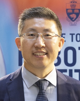
Yu Sun |
|
Professor |
|
Lifetime Fellow, Canadian Academy of Engineering (CAE) |
| Department of Mechanical and Industrial Engineering |
| University of Toronto |
|
Canada |
|
Personal homepage |
|
|
|
Title: Microsystems for Manipulating and Characterizing Cells and Tissues |
|
Abstract: The capability of manipulating micro and nanometer-sized objects, such as cells and nanomaterials opens new frontiers in robotic surgery, disease diagnostics, industrial applications and enables new discoveries in many disciplines such as biology, medicine, and materials science. The field of micro-nanorobotics involves the design and construction of robotic agents that are micro-nanometer sized and robotic manipulation of objects with dimensions in the micrometer and nanometer ranges. The past two decades has witnessed spurred development of micro-nanorobotic systems and technologies with common hallmarks of precision instrumentation, sensing, actuation, and control. This talk will begin with a brief review of the evolution of the robotic micromanipulation field, followed by an overview of challenges, opportunities, and recent advances made in this field. Examples of robotic cell manipulation systems for clinical surgery and drug screen will be given, and sub-micrometer position control and sub-nanoNewton force control for realizing 3D intracellular and intra-tissue manipulation and measurement will be introduced. |
|
|
|

|
|
Kristina Tschulik |
|
Professor |
|
Chair of Analytical Chemistry II |
| Electrochemistry and Nanoscale Materials |
| Ruhr-University Bochum |
|
Germany |
|
Personal homepage |
|
|
|
Title: Nanoelectrochemistry: Unravelling nanoparticle (re-)activity by single nanoparticle electrochemistry |
|
Abstract: Nanomaterials have been in the focus of major research interest for more than two decades. The great potential of electrochemistry to characterize these particles in terms of both, their physical properties and chemical reactivity, however, has hardly been explored. The ease of sample preparation, the comparably high speed and low cost of nano-electrochemistry, make it a useful complement or even alternative to the established nanoparticle characterization methods, like SEM or TEM. The number of particles that can conveniently be analysed, ranges from individual ones to ensembles comprising myriads of nanoparticles, depending on the techniques use. In this talk, several examples will be presented.
A convenient method for nanoparticle sizing in their native environment is via transformative nano-impact analysis.[1] This methodology uses the Brownian motion-based sporadic impact of dispersed nanoparticles at a potentiostated electrode to electrochemically convert one particle at a time. The charge transferred during this conversion can, for instance, be used to size the particle or to determine its composition. Measuring the electrocatalytic activity – likely the most frequently used electrochemical nano-ensemble studies – may also be realized at the single particle level. This is presented for the oxygen evolution reaction (OER) at mixed transition metal oxide nanoparticles at extremely high current density and turn-over-frequencies orders of magnitude higher than achieved in conventional studies.[2,3]
Last but not least, individual particle reactivity studies at surface-immobilized particle ensembles will be introduced. This will be shown for Ag and Au nanoparticles by dark-field microscopy coupled to hyperspectral imaging in different liquid surroundings.[4] |
|
|
|

|
|
Joseph Wang |
|
Distinguished Professor |
|
SAIC Endowed Chair |
| Department of Nanoengineering |
| University California San Diego (UCSD) |
|
USA |
|
Personal homepage |
|
|
|
Title: Microrobots Go in-vivo: From Test-tubes to Live Animals |
|
Abstract: Nanoscale robots that can effectively convert diverse energy sources into movement and forces represent a rapidly emerging and fascinating robotic research area. Such nanoscale robots offer impressive capabilities, including greatly enhanced power and cargo-towing forces, multi-functionality, easy surface functionalization, and versatility. The new capabilities of modern nanorobots indicate immense potential for a variety of biomedical applications, and should have major impact on disease diagnosis, treatment, and prevention [1]. Recent in vivo applications using different types of biocompatible and biodegradable microrobots will be illustrated, including enhanced drug delivery towards enhanced treatment of stomach bacterial infection, active vaccine delivery, autonomous gastric fluid neutralization, the ability to selectively localize at desirable segments of the GI tract, or efficient intracellular delivery of functional proteins and nucleic acids.
|
|
|
|

|
|
Quan Zhou |
|
Professor |
|
Department of Electrical Engineering and Automation |
|
| Aalto University |
|
Finland |
|
Personal homepage |
|
|
|
Title: Manipulation and Assembly of Particles using Acoustic Field Gradient and Electromagnetic Needle |
|
Abstract: Robotic instruments are miniature robots and mechatronic systems that can manipulate small objects and precisely interact with different surfaces. In this talk, I will discuss our recent work in robotic instruments for manipulation and assembly of particles using two techniques: acoustic manipulation devices that can automatically manipulate/assembly/shaping a large amount of particles on a surface using the field gradient generated by a single acoustic transducer, both in ambient air and submerged; and robotic electromagnetic needles that can precisely extract and independently manipulate/assemble magnetic microparticles in the presence of neighboring magnetic particles by contact or contactless. Additionally, I will discuss electromagnetic needle induced active magnetic fluid manipulator that can manipulate particles on the air-liquid interfaces. |
|
|
|
|
Li Zhang |
|
Professor |
|
Department of Mechanical and Automation Engineering |
|
Chow Yuk Ho Technology Centre for Innovative Medicine
CUHK T Stone Robotics Institute |
The Chinese University of Hong Kong (CUHK) |
|
China |
|
|
|
|
|
|
|
Title: Bio-inspired Magnetic Microrobots: From Individual to Swarm |
|
Abstract: People have envisioned tiny machines and robots that can explore the human body, find and treat diseases since Richard Feynman’s famous speech, “There's plenty of room at the bottom,” in which the idea of a “swallowable surgeon” was proposed in the 1950s. Even though we are at a state of infancy to achieve this vision, recent intense progress on nanotechnology, MEMS/NEMS technology and micro-/nanorobotics has accelerated the pace toward the goal. A number of research efforts have been recently published regarding the development of tiny swimming machines/robots from the basic principles and fabrication methods to practical applications. | |
*The list of Keynote speakers is based on the alphabetical order of family names
|
|
|
