|
|
| |
Keynote Speakers |
|
|
|
|
|
|
|
| |
|

|
|
Poul M. Bendix |
|
Associate Professor |
|
Niels Bohr Institute |
|
| University of Copenhagen |
|
Denmark |
|
Personal homepage |
|
|
|
Title: Interregation of cell surface dynamics by using optical manipulation and thermoplasmonics |
|
Abstract: Investigations of cell surface dynamics is experimentally challenging due to the dynamic nature of nanoscopic surface structures having complex 3D shapes. The cell surface environment exhibits constant shape changes driven by molecular complexes in the membrane and by supporting cytoskeletal structures. Molecular shapes and cooperativity are emerging as important functional properties of cells to support formation of essential nanostructures on the cell surface. Membrane proteins with bent shapes can sense curvature cues and undergo crystallization at high density which could play a regulatory role in a number of cell functions and cellular disorders. Here, I will present quantitative studies on cell surface dynamics using optical force sensing and present a new thermoplasmonic technique for fusion of cells and for nanoscopic perturbation of the cell membrane. Plasmonic heating from optically trapped nanoheaters causes, in vivo-like, nanoscopic injuries to living cells and is paralleled by confocal microscopy to detect the molecular response. Optical manipulation, combined with protein expression in living cells and in isolated plasma membrane vesicles, allows us to quantify the correlation between molecular shapes and curvature sensing at the internal side of the plasma membrane. With these novel experiments, we gain a new understanding of the mechanisms governing cell surface protein dynamics and mechanical properties of the surface of living cells.
|
|
|
|

|
|
Yang Chai |
|
Assistant Professor |
|
Department of Applied Physics |
|
| The Hong Kong Polytechnic University |
|
China |
|
Personal homepage |
|
|
|
Title: Two-Dimensional Layered Materials for Nanoelectronics |
|
Abstract: As the Moore’s law is coming close to its end, the development of future semiconductor research requires low power and high performance nanoelectronics (More Moore) and diverse and multifunctional devices (More than Moore). It has been becoming inevitable to introduce new materials into the existing Si platform to augment its functions. Two-dimensional layered semiconductors possess ultrathin body, atomic scale smoothness, dangling bond-free surface, reasonable good mobility, and sizable bandgap, which enable promising applications in nanoelectronics. Recently, we used graphene as the barrier of the Cu interconnect to replace conventional TaN barrier. Our experimental and computational results show that graphene barrier can meet the ITRS requirement. We also reveal distinct growth dynamics of semiconducting MoS2 flakes using in-situ transmission electron microscopy, and demonstrate a systematic study on group-10 transition metal dichalocogenides. |
|
|

|
|
Tawfique Hasan |
|
Reader in Nanomaterials Engineering |
|
Cambridge Graphene Centre |
|
| University of Cambridge |
|
UK |
|
Personal homepage |
|
|
|
Title: Formulation and Manufacturability of 2D Material Functional Inks and Devices |
|
Abstract: Beyond graphene, non-carbon two-dimensional (2D) crystals have recently shown huge promises for applications in a wide range of optoelectronic devices. Solution processability of these materials offers an exciting opportunity when applications with large form factors are envisaged. As an inevitable extension to the requirements of solution processability, the ability to formulate their functional inks is of paramount importance for large-scale device manufacturability. I will introduce inkjet printable ink formulation of graphene, transition metal dichalcogenides (TMDs) and black phosphorus (BP). First, I will briefly discuss printed sensors and flexible thermoelectric generators using inkjet printed graphene. For TMDs and BP, I will demonstrate the importance of using a mixed solvent approach in ink formulation to achieve excellent print quality. This, in addition to the choice of solvents enable reliable inkjet printing for scalable device development, even for wafer-scale device arrays. Our approach to formulate these functional inks could also be exploited to develop functional inks of other 2D materials for large-scale manufacturability. |
|
|

|
|
Seng-Tiong Ho |
|
Professor |
|
Electronical and Computer Engineering |
|
| Northwestern University |
|
USA |
|
Personal homepage |
|
|
|
Title: Physics and Technologies of Micro/Nano Lasers |
|
Abstract: Micro and nano lasers are of interest for potential applications to on-chip sensing, imaging, optical interconnects, and various other areas. In this talk, I will review the physics and technologies involved in such lasers. Micro and nano lasers have properties that distinguish them from typical lasers due to their microscopic optical cavities. I will discuss what they are. I will then describe the idea of thresholdless lasers and light source with ultrafast modulation capability. Micrometer-scale and nanometer-scale (micro/nano) lasers, when properly designed, can take advantage of the unique capabilities of microcavity lasers. There are various approaches to realizing microscale or nanoscale microcavity lasers. I will describe some of the early realization of micro/nano lasers that include VCSELs, microdisk lasers, and photonic-wire or microring lasers. I will then discuss more recent realization of micro/nano lasers that include photonic crystal lasers and plasmonic waveguide based lasers. I will summarize and compare the properties of these micro/nanolasers and discuss their application interests.
|
|
| | |
|

|
|
Mark Hopkinson |
|
Professor |
|
Department of Electronic and Electrical Engineering |
|
|
|
University of Sheffield |
|
UK |
|
Personal homepage |
|
|
|
Title: In-situ laser interference surface patterning of nanomaterials |
|
Abstract: The development of new methods for the production of large scale arrays of identical nanostructures is of vital importance for the future development of electronic, photonic and biological materials. The conventional methodology of lithographic processing and etch has served us well for many decades, but is now becoming compromised by economic and technology limitations as we seek sub-10nm dimensions. As an alternative approach, self- assembly methods have shown the capability to form nanostructures with well-defined properties and novel functionality (eg: quantum dots). However, the lack of size selectivity and site control is a major limitation of such approaches. To progress with self-assembly, we require in-situ methods which can control the nucleation site to produce an addressable ensemble of structures with identical structure.
The presentation will review work performed under the EU program Nanostencil3on the in-situ laser interference processing of materials. Our approach is based on the well-established potential of laser interference lithography to pattern a regular grid in a single pulsed exposure. The project seeks to apply this approach to materials processing reactors within which we interact with the surface at the materials formation stage. The methods include Molecular Beam Epitaxy, Chemical Vapour Deposition and surface oxidation reactions. We seek to nucleate self-assembled nanostructures at precise sites patterned by interferometric light by exploiting the photothermal photochemical modification of the surface. The talk will discuss the potential of this method and early stage proof of principle of its potential. |
|
|

|
|
Chaoyuan Jin |
|
Professor |
|
College of Information Science & Electronic Engineering |
|
| Zhejiang University |
|
China |
|
Personal homepage |
|
|
|
Title: Cavity-enhanced nanophotonic switching |
|
Abstract: The power consumption of signal switching/routing is considered to become a serious bottleneck in scaling up the bandwidth for short-reach communications. The development of high-performance, energy-efficient photonic devices is therefore crucial in tackling this problem. To achieve the energy efficient goal, we have reviewed the fundamental limitation of semiconductor-based switching devices and find out there are general ways to further scale down the energy consumption at ultrafast operation speed, for example, by increasing the field confinement of photonic cavities, leading to the ultrafast control of cavity quantum electrodynamics. Recent demonstrations of nanostructure-based photonic devices are discussed with a particular focus on the real-time control of cavity field, which provides an extra degree of freedom to manipulate radiative processes which are key to classical and quantum photonic devices. In quantum information systems based on photon exchange between semiconductor-based quantum nodes, the processes of photon emission and absorption is controlled in a time-scale shorter than the radiative lifetime. In nanophotonic devices, ultrafast laser sources and photonic switches are either demonstrated by controlling the carrier dynamics in semiconductors or by the ultrafast modulation of cavity properties.
|
|
|
|

|
|
Jong Min Kim |
|
Professor |
|
Department of Engineering |
|
| University of Cambridge |
|
UK |
|
Personal homepage |
|
|
|
Title: |
|
Abstract: |
|
|

|
|
Viktor Koledov |
|
Professor |
|
Head |
| Magnetic Phenomena Laboratory |
| Kotelnikov IRE RAS |
|
Russia |
|
Personal homepage |
|
|
|
Title: Nano-Manipulation, Nano-Manufacturing, Nano-Measurements by New Smart Material-Based Mechanical Nanotools |
|
Abstract: Recent progress in the study of new functional materials, such as Ti(NiCu) intermetallic with shape memory effect (SME), opens up exciting possibilities for the design reconfigurable micro- and nano-structures and for operating mechanical nanotools controlled by external fields or heat. This report gives an overview of physical effects, in particular, solid state phase transitions and accompanying phenomena in alloys and composites exhibiting SME. The limitations pertaining to the minimum size of the nanomechanical devices exhibiting shape memory effect that arise due to the solid state phase transitions are now under discussion and have not been completely understood yet. The modern nanotechnologies allow designing of the mechanical micro- and nanotools, such as nanotweezers, nanopinchers etc., with an active layer thickness of about several tenths of nm, and whose overall size is below 1 μm. The nanotools with SME can be controlled by heating as well as by magnetic field activation in ferromagnetic alloys exhibiting SME, such as Ni2MnGa. 3D nanomanipulation is demonstrated by composite nanotweezers with SME in different nanoobjects, such as CNTs, nanowires, nanowhiskers, bionanoobjects, DNA, etc. In these devices, the surface interactions and Casimir and van der Waals forces affect the process of nanomanipulation. The prospects of nanorobotics and manufacturing on nanoscale adapting the principle of mechanical bottom-up nanoassembly are discussed. In addition, nanoscale measurements can take advantage of 3D mechanical nanomanipulation, including transportation of analytes to nanosensors, elasticity measurements by nanotools with calibrated force, etc. |
|
|
|

|
|
Erkki Levanen |
|
Professor |
|
Head of Research Group |
|
| Tampere University of Technology |
|
Finland |
|
Personal homepage |
|
|
|
Title: Green, supercritical CO2 assisted processing of functional surfaces |
|
Abstract: There is urgent need for manufacturing of complex structures and large surfaces with sustainable ways and supercritical CO2 assisted processing techniques will offer one promising way to produce ceramic nanoparticles and well-defined ordered structures and surface topographies. TiO2 and Zn-based materials are possible to produce by hybrid manufacturing technologies combining e.g. sol-gel, ablation and chemical growth in CO2 environment. This study sustainable manufacturing routes of functional ceramics and their structure and properties. |
|
|

|
|
Jack (Jikui) Luo |
|
Professor |
|
Institute for Materials Research and Innovation |
|
| The University of Bolton |
|
UK |
|
Personal homepage |
|
|
|
Title: Flexible electronics for medical and healthcare applications |
|
Abstract: Flexible electronics is an emerging technology, that can be applied to a range of biomedical and wearable applications. Flexible electronics possesses some unique properties such as excellent conformability, stretchability and wearability that rigid electronic counterparts are unable to provide. Owing to its great potential for widespread applications, many flexible electronic devices and technologies have been developed and their applications been explored.
This talk will introduce a number of flexible electronic technologies we developed, including stretchable/bendable skin-like sensors for touch/strain/force/temperature detection; flexible planar ECOG with hundreds of electrodes; wearable wireless sensor chips etc for biosensing, implant and wearable applications; and unique flexible surface acoustic wave (SAW) resonators and film bulk acoustic resonators (FBAR) for biosensing and microfluidics applications. The skin-like sensors possess multiple-sensations for temperature, touch, pressure and shape with the pressure sensitivity better than human skins, and those finger-type flexible sensors can fit on the fingers of a robot to perform force-feedback gripping and objective separation etc. SAW on rigid piezo-substrate has utilized in microfluidics/lab-on-chip applications to transport/mix pl-l volume liquids, generate droplets, perform cell separation/identification, cell lysis with excellent result, while the new flexible acoustic resonator sensors are able to perform some of the functions under a bending condition with high sensing sensitivity that are compatible to or better than those of rigid counterparts, showing a great potential for applications in environmental and health monitoring, performance enhancement etc.
|
|
|
|
|
|
Zhengtang Luo |
|
Assistant Professor |
|
Department of Chemical & Biological Engineering |
|
| Hong Kong University of Science and Technology |
|
China |
|
Personal homepage |
|
|
|
Title: Chemical Vapor Deposition Growth of Two Dimensional Materials for Electronic Devices and Energy Applications |
|
Abstract: The discovery of graphene has promoted an extensive research on a variety of two-dimensional materials comprising hexagonal boron nitride (h-BN), transition metal dichalcogenides (TMDs) and others, which expanded the 2D materials family over the years. Consequently, the 2D materials family provides a wide flavor of electronic properties generating wide bandgap insulators, semiconductors, semimetals and metals. Therefore, the unique characteristics of 2D materials urge them as potential candidate for a broad spectrum of applications including optoelectronic devices, biosensing, electrocatalysis and many others. Our research group has been working on the synthesis and functionality of these 2D materials for a substantial time period. In this talk, I will present our recent work on the carbon gettering approach for chemical vapor deposition (CVD) growth of high-quality millimeter sized single crystal graphene for the optoelectronic applications. Further, I will discuss the CVD growth of a variety of TMDs materials and their heterostructures, which we have demonstrated to have great potential for photodetectors and other energy related applications. |
|
| | |
|

|
|
Bill Milne |
|
Emeritus Professor |
|
Engineering Department |
|
| University of Cambridge |
|
UK |
|
Personal homepage |
|
|
|
Title: FBAR devices for Gravimetric and Bio-Sensing applications |
|
Abstract: This talk will describe the design and development of Gravimetric and Biological Sensors based on thin Film Bulk Acoustic Resonator (FBAR) Technologies. The FBAR devices were fabricated mostly on ZnO nanocrystalline thin films deposited using a novel High Target Utilisation Sputtering System (HiTUS). The system ensures that we can produce low stress films at the high deposition rates necessary for such structures to operate efficiently. We will describe gravimetric sensors based on such sensors, and end with a description of our more recent results on dual mode thin film FBARs for parallel sensing of both mass loading and temperature. |
|
|

|
|
Adrian Neild |
|
Professor and Australian Research Fellow |
|
Director of Research |
|
Department of Mechanical and Aerospace Engineering |
| Monash University |
|
Australia |
|
Personal homepage |
|
|
|
Title: Microfluidic Manipulation of Nanoparticles and Nanolitre Volume Droplets |
|
Abstract: Surface acoustic waves have proved a very promising way to interact with fluid enclosed in microfluidic systems. The coupling of sound waves into the fluid, from a piezoelectric substrates, allows forces to be exerted on suspended matter, fluids and interfaces, these allow tasks such as cell patterning, fluid mixing and droplet generation to be performed. In this work, the potential for controlling droplets in a microfluidic network will be explored, performing such tasks as droplet steering, merging and subdivision. In addition the nature of the interaction of such waves with particles of different sizes will be examined, giving new incite into the nature of the sound fields created and their potential for capturing nanoparticles. |
|
|
|

|
|
Shunri Oda |
|
Professor |
|
|
Tokyo Institute of Technology |
|
|
Japan |
|
Personal homepage |
|
|
|
Title: Low Dimensional (0D, 1D, 2D) Devices for Future Electronics |
|
Abstract: One of the major application targets for future electronics is wearable communication tools with low-power consumption. Tunnel field-effect-transistors (TFET) are promising since extremely low-voltage operation of switching beyond the limitation of CMOS devices would be possible. 2D materials and 1D nanowires attract attention not only because these materials would be suitable for the fabrication of TFETs, but also various novel application such as sensors, displays would be possible. Quantum computing is no longer a future technology. Recent advances in D-Wave computers based on quantum annealing and superconducting devices, and the demonstration of long spin decoherence times in isotopically-enriched Si qubits, have accelerated the research and development of this technology. The remaining challenge is large scale integration of qubits. Physically-defined coupled quantum dots (QDs) on silicon-on-insulator substrates are promising for multiple scaled qubits. In this paper, we discuss recent progress of 0D (quantum dots), 1D (nanowires) and 2D atomic-layer materials devices. |
|
|
|

|
|
Seeram Ramakrishna |
|
Professor |
|
Director |
| Center for Nanofibers & Nanotechnology |
| National University of Singapore |
|
Singapore |
|
Personal homepage |
|
|
|
Title: Functional Nanofibers |
|
Abstract: Product innovations as well as manufacturing innovations are closely related to the materials innovations. Together they enable better living – clean air, water and energy, health and wellbeing, smart living and transportation, safety and security, and circular economy. Functional nanomaterials and materials informatics are emerging domains of materials innovation. Electrospinning has been developed as a viable manufacturing method for producing a range of nanofibers and nanoparticles of polymers, metals, ceramics, carbon, and their combinations. It has also evolved into a 3D printing or additive manufacturing method. Functional nanomaterials enable air filtration, water purification, clean energy generation and storage, controlled drug delivery, tissue engineering, regenerative medicine, food packaging, high performance apparel, electronic-skin, wearables, and light-weight, damage tolerant materials for transportation, electricity transmission, buildings and construction. They also enable self-cleaning, super-hydrophilic, super-hydrophobic, and anti-microbial surfaces. Materials Informatics approach based on advances in machine learning is developed to mine properties of nanomaterials. This lecture provides an overview, and discusses emerging opportunities.
|
|
|
|

|
|
Krishnan Venkatakrishnan |
|
Professor |
|
Department of Mechanical and Industrial Engineering |
|
Ryerson University |
| Canada |
|
|
|
Personal homepage |
|
|
|
Title: Beyond Nanoscale – A Next Generation Biocompatible Pathway for Analytical Bio-sensing and Cancer Diagnostics & Imaging |
|
Abstract: Quantum/ Nano scaled materials engineered with multi-photon ionization interaction can be programmed to generate multiple phased structures as well as varied morphologies in order to obtain unique optical and biochemical properties that have never been observed before. Using femtosecond laser ablative synthesis, the quantum and nano materials was created for ultrasensitive cancer diagnostics, label-free fluorescence imaging as well as cancer therapy. The materials are able to behave like an extra-cellular matrix for cell adhesion and proliferation for in-vitro analysis. Our focus is to synthesize bio-compatible and non-plasmonic materials like silicon, graphene, nickel, titanium, zinc etc. Current study focuses on the apoptotic pathways on cancer cells and the selective behavior of the materials, which allow enhancement of proliferation for fibroblasts. Substantial SERS enhancement was obtained from the typically non-Raman active materials. Single cell level sensitivity was achieved and biomolecules like DNA, RNA, Proteins, lipids of alive cell was detected. In addition, the femtosecond laser synthesized three dimensional structures show very high quantum yield. A label free fluorescence imaging platform was developed thanks to the enhanced absorption and fluorescence throughput of the quantum structures . Our research in this direction may open up new possibilities for ultra-sensitive cancer diagnosis. |
|
|
|
|
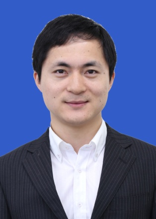
Zhonglin Wang |
|
Professor |
|
Beijing Institute of Nanoenergy and Nanosystems |
| Chinese Academy of Sciences, China |
|
School of Materials Science and Engineering
Georgia Institute of Technology |
|
USA |
|
Personal homepage |
|
|
|
Title: Nanogenerator for self-powered systems, IoTs, artificial intelligence and blue energy |
|
Abstract: Self-powered system is a system that can sustainably operate without an external power supply for sensing, detection, data processing and data transmission. Nanogenerators (NG) were first developed for self-powered systems based on piezoelectric effect and triboelectrification effect for converting tiny mechanical energy into electricity, which have applications in internet of things, environmental/infrastructural monitoring, medical science, environmental science and security. Here, we first present the fundamental theory of the NGs starting from the Maxwell equations. In the Maxwell’s displacement current proposed in 1861, the term E ∂E/∂t gives the birth of electromagnetic wave, which is the foundation of wireless communication, radar and later the information technology. Our study indicates that, owing to the presence of surface polarization charges present on the surfaces of the dielectric media in NG, an additional term (∂P_s)/∂t should be added in the Maxwell’s displacement current, which is the output electric current of the NG. Therefore, our NGs are the applications of Maxwell’s displacement current in energy and sensors. NGs have three major application fields: micro/nano-power source, self-powered sensors and blue energy. We will present the applications of the NGs for harvesting all kind mechanical energy that is available but wasted in our daily life, such as human motion, walking, vibration, mechanical triggering, rotating tire, wind, flowing water and more. Then, we will illustrate the networks based on triboelectric NGs for harvesting ocean water wave energy, for exploring its possibility as a sustainable large-scale power supply. Lastly, we will show that NGs as self-powered sensors for actively detecting the static and dynamic processes arising from mechanical agitation using the voltage and current output signals. |
|
|
|
|
|
Dong Wu |
|
Professor |
|
Micro&Nano Engineering Laboratory |
| School of Engineering Science |
| University of Science and Technology of China |
|
China |
|
Personal homepage |
|
|
|
Title: SLM-based high-efficiency 3D Femtosecond laser microfabrication for microoptical and microfluidic applications |
|
Abstract: Femtosecond laser induced two-photon polymerization (TPP) has been proved to be a powerful microfabrication technique with high efficiency and quality. However, the main drawback of TPP technique is its low fabrication efficiency caused by the point-to-point raster scanning strategy, which seriously restricts its applications. In order to overcome the disadvantages, SLM-based (spatial light modulator) 2D-3D laser intensity patterns (e.g., mutlifoci or arbitrary patterns) were proposed to significantly speed up the fabrication process by serveral orders of magnitude, and has a wide range of applications in optics, micromachines, and biology, owing to its capability to dynamically update the intensity distributions in the focal plane by modifying the phase of incident light. A series of 2D-3D functional microdevices such as Damman grating, microfilter and flower-like microtube arrays were rapidly fabricated and show various functions, such as beam splitting, particles filtering and cell manipulation.
|
|
|

|
|
Jungwon Yoon |
|
Associate Professor |
|
School of Integrated Technology |
| Gwangju Institute of Science and Technology (GIST) |
|
|
Korea |
|
Personal homepage |
|
|
|
Title: Non-invasive Electromagnetic Guidance Schemes of Magnetic Nanoparticles for Drug Delivery to a Brain |
|
Abstract: Electromagnetic sensing and guidance schemes using magnetic nanoparticles(MNPs) can allow a nanotechnology-based drug delivery approach to be feasible for potential therapies for neurodegenerative diseases such as Alzheimer's disease. In this talk, I will introduce an electromagnetic guidance scheme of magnetic nanoparticles without particles’ aggregation to deliver them to a brain efficiently, then show how the magnetic particle imaging (MPI) scheme for the particles’ monitoring can be combined with the electromagnetic guidance scheme. The proposed guidance approaches can be adapted to a medical robotic platform for brain drug targeting, brain stimulation, and brain hyperthermia. |
|
|
|
|
Li Zhang |
|
Associate Professor |
|
Department of Mechanical and Automation Engineering |
|
The Chinese University of Hong Kong (CUHK) |
|
Hong Kong SAR |
|
China |
|
|
|
|
|
Title: Microrobotic Swarm: Reconfigurable Pattern Generation and Motion Control
Abstract: To control a swarm of microrobots with external fields is one of the major challenges for untethered microrobots. In this talk, I will present generation of reconfigurable paramagnetic nanoparticle based microswarm, using dynamic magnetic fields. The nanoparticle swarm exhibits a dynamic-equilibrium structure, in which the nanoparticles perform synchronised motions in fluid. By tuning the input parameters of the dynamic magnetic field, the pattern of the magnetic swarm is capable of performing reversed transformation, such as swelling and shrinkage. Moreover, reversible merging and splitting of the swarms are demonstrated and investigated. Serving as a mobile robotic end-effector, the swarm is capable of making locomotion by tuning the pitch angle of the actuating field. In addition, localized delivery will be demonstrated. Finally, the opportunities and challenges of magnetic microrobotic swarm for biomedical applications will be discussed. |
| | | | |
|
|
|

