|
|
| |
Keynote Speakers |
|
|
|
|
|
|
|
| |
 |
|
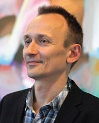
Peter Bøggild |
| Professor |
| DTU Nanotech |
|
Department of Micro-and Nanotechnology |
|
Technical University of Denmark |
|
Personal homepage |
| Title: 2D or not 2D: Electrical Continuity of Graphene and How to Measure It |
|
Abstract: For nearly all applications of large-area graphene, the presence of cracks, rips, holes and tears is unacceptable. In this work, several non-destructive, large-area characterization techniques, including micro four-point probe and Terahertz time-domain spectroscopic conductance mapping, as well as gigapixel quantitative optical microscopy are for the first time combined to study the electrical continuity of chemical vapor deposited graphene on length scales from 100 nm to 100 um. We investigate how catalyst crystallinity, domain size distribution, growth parameters as well as the transfer process, affect the chance of making truly two-dimensional graphene. |
|
|
 |
|
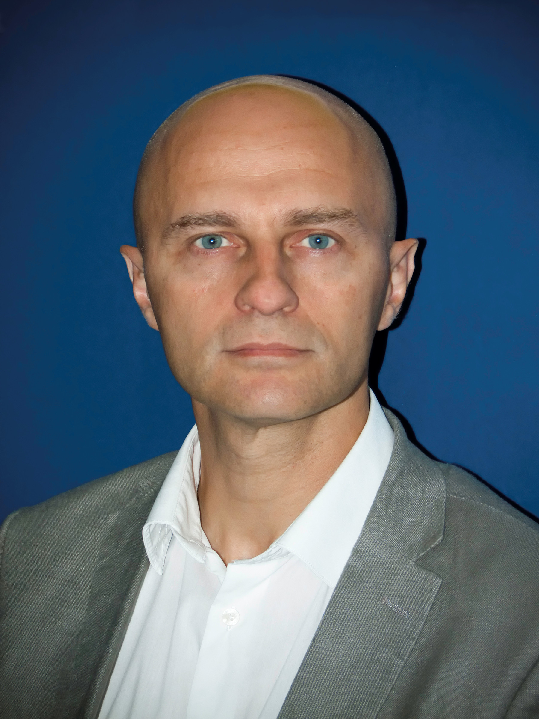
Lionel Buchaillot |
| Professor |
| University of Lille Nord de France |
|
Director |
|
The Institute of Electronics, Microelectronics |
| and Nanotechnology - IEMN |
| France |
|
Personal homepage |
| Title: Ultimate Ring Resonator for Atomic Force Microscopy: A Possible Way |
| for Biosensing |
|
Abstract: Since its discovery, atomic force microscopy (AFM) has paved the way for new research experiments in physics allowing multi physics probing combined with ultimate imaging at the atomic scale. Microlevers tapered by metal or active materials have allowed unprecedented experiments leading to original electrical, mechanical and magnetic measurements, among others. It has been now more than 10 years since biologists started paying attention to this wonderful instrument. At the early stage, they were satisfied by the AFM characteristics, but now, they expect better performances not only in air, but in liquid medium as well. In order to comply with this requirements, we designed a ring resonator featuring interesting data for biosensing, e.g. the ability to operate the probe at very high frequency compare to standard AFM levers. |
|
|
 |
|
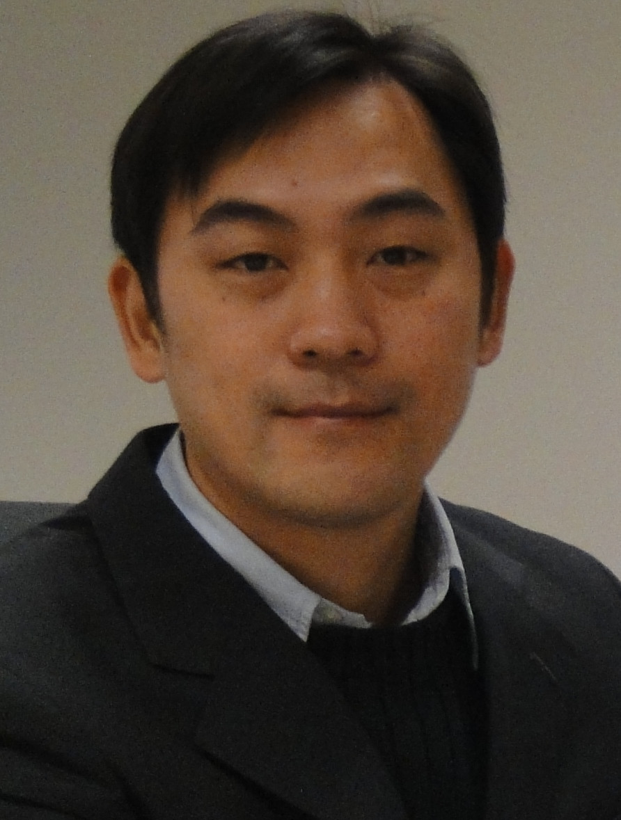
Chih Wei Chu |
|
Associate Research Fellow |
| Research Center for Applied Sciences |
|
Academia Sinica |
|
Associate Professor |
| Department of Photonics |
| National Chiao-Tung University |
|
Personal homepage |
| Title: Nanostructure Conducting Polymer for Energy-Related Applications |
|
Abstract: Conjugated organic materials, possessing electrical and optical properties similar to metals and inorganic semiconductors, are capable of bringing new opportunities because of their soft nature, and thus allowing high flexibility. Poly (3, 4-ethylenedioxythiophene): Polystyrene sulfonate (PEDOT: PSS) and Poly (3, 4-ethylenedioxythiophene) (PEDOT) have been investigated most often because of their reasonable electric conductivity, low oxidation potentials, biocompatibility, and environmental stability at high temperature. In this presentation, I will introduce different facile approaches to enhance conductivity of PEDOT: PSS and fabricate nanostructure PEDOT films as well as their energy-related applications. |
|
|
|
 |
|
Andreas Dietzel |
| Professor |
| Institute of Microtechnology |
|
Braunschweig University of Technology |
|
Germany |
|
Personal homepage |
| Title: Miniaturized Systems for Pharmaceutical and Medical Applications |
|
Abstract: Micro-/Nanotechnologies offer many advantages over conventional systems in particular in the field of health care applications. Several examples such as point of care sensors including elements of fluid manipulation and sensing within a single chip, mechanically flexible microsystems that allow more comfortable adaption to the shape of the human body to be used for monitoring, and systems for the processing and formulation of nano-particulate pharmaceuticals for the small scale production of individualized medicine will be discussed. |
|
|
 |
|
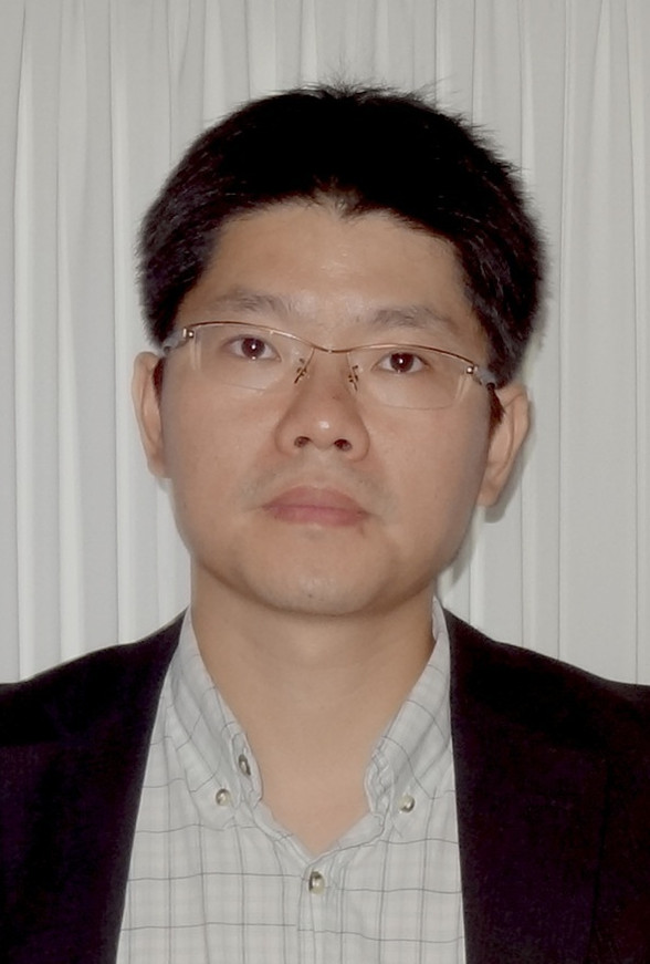
Mingdong Dong |
| Assoc. Professor |
| Head, Bio-SPM Lab |
|
Interdisciplinary Nanoscience Center (iNANO) |
|
Aarhus University, Denmark |
|
Personal homepage |
| Title: Multiparametric Imaging of Nanomaterials by Dynamic Quantitative |
| Nanomechanical Mapping |
|
Abstract: Force spectroscopy is a powerful method to measure physical properties of materials. Recently progress has been made in the characterization of nanomechanical properties using Dynamic Quantitative Nanomechanical Mapping (DQNM). DQNM has the ability to recover the tip–sample force waveforms which provide high-speed force–distance curves and allow specific material properties to be measured with high spatial resolution. This talk will review the recently developed experimental technique and its applications in quantitative imaging of biological molecules and nano materials. |
|
|
 |
|
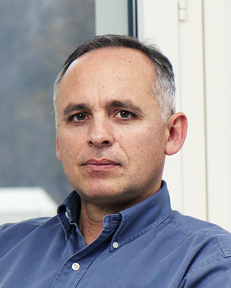
Evangelos S. Eleftheriou |
| PhD, IBM Fellow |
| Head, Storage Technologies Department |
|
IBM Zurich Research Laboratory |
|
Switzerland |
|
Personal homepage |
| Title: Key Enabling Technologies for Scanning Probe Microscopy |
|
Abstract: Manipulation and interrogation at the nanometer scale with a scanning probe microscope (SPM) necessitate high-resolution sensing and positioning systems with atomic-scale accuracy. This talk will review recent progress in cantilever-deflection sensing for atomic force microscopy (AFM) using nonoptical means, including schemes suitable for multi-resolution imaging. A second focus will be a key enabling technology for SPM, namely, nanopositioning, and discuss four technology elements that are vital for high-speed nanopositioning: (1) a magnetoresistance-based high-bandwidth and low-noise nanoscale sensing scheme, (2) dual-stage nanopositioners, (3) noise-resilient feedback controllers using hybrid control, and (4) optimized scan trajectories. |
|
|
 |
|
Weileun Fang |
| Distinguished Professor |
| Head, Micro Device Laboratory |
|
Power Mech. Eng. Dept. and NEMS Institute |
| National Tsing Hua University |
|
Personal homepage |
| Title: CMOS MEMS: A Key Technology Towards the “More Than Moore” Era |
|
Abstract: The mature CMOS fabrication processes are available in many IC foundries. It is cost-effective to leverage the existing CMOS fabrication technologies to implement MEMS devices. On the other hand, the MEMS devices could also add values to the IC industry as the Moore’s law reaching its limit. The CMOS MEMS could play a key role to bridge the gap between the CMOS and MEMS technologies. The CMOS MEMS also offers the advantage of monolithic integration of ICs and micro mechanical components. This talk introduces the approach to implement and integrate various MEMS transducers by leveraging standard CMOS processes. Note that other process platforms (e.g. poly-Si, CNT, glass, metal, etc.) are also of importance for different MEMS applications. In future, these process platforms could enhance the variety and performance of on-chip devices as moving towards the “More than Moore” era. |
|
|
 |
|
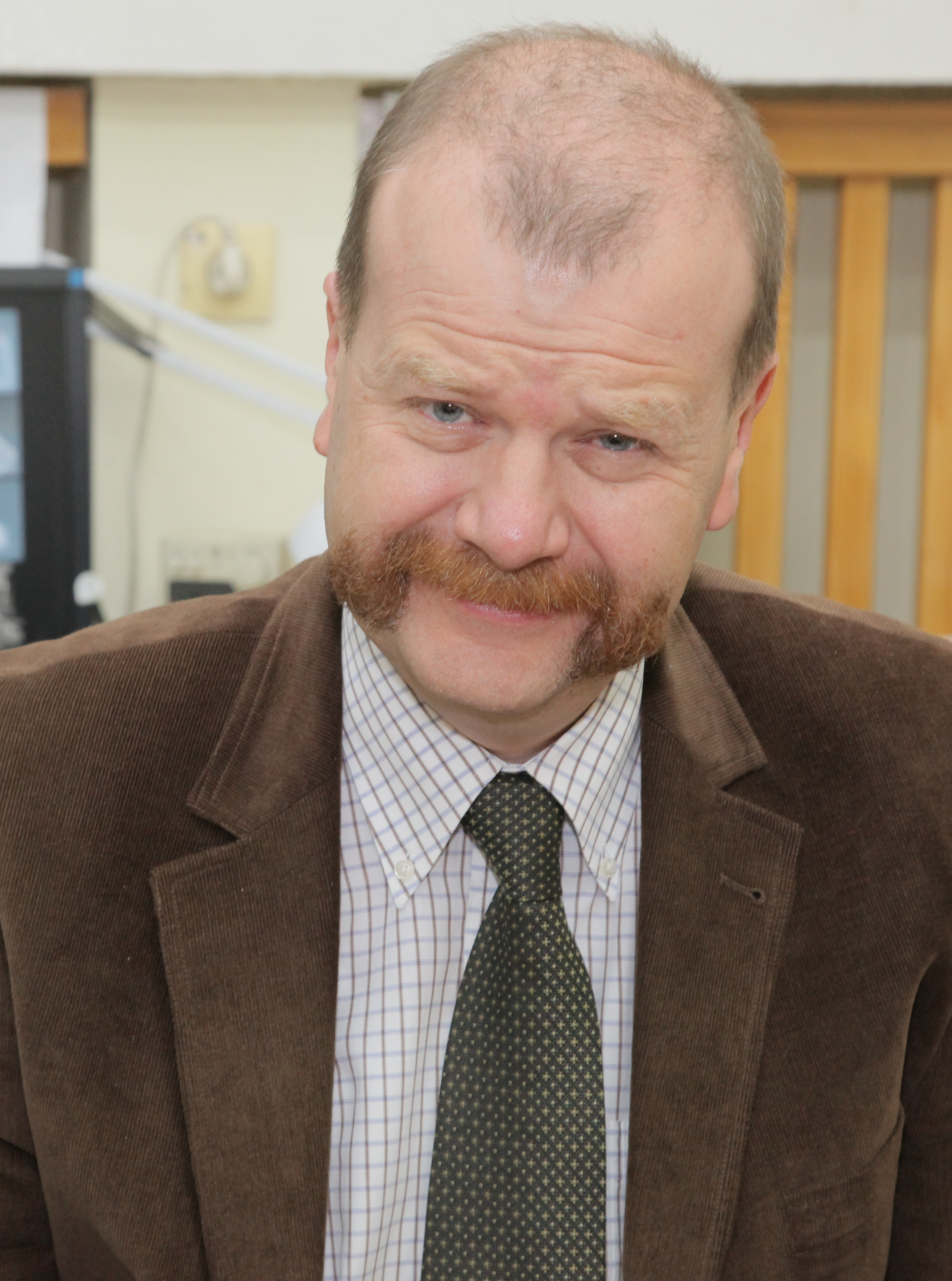
Teodor Pawel Gotszalk |
| Professor |
| Head, Nanometrology Lab |
|
Faculty of Microsystem Electronics and Photonics |
|
Wroclaw University of Technology, Poland |
|
Personal homepage |
| Title: Nanometrology Using Scanning Probe Microscopy Methods |
|
Abstract: Scanning probe microscopy (SPM) belongs to the high resolution methods for imaging of micro- and nanostructures. This technology has been used successfully in the university and industry research laboratories for over two decades. Despite progress in this field a lot of effort must be done in order to enable quantitave (in other words metrological) surface investigations. In this presentation latest results on metrological applications of the SPM related methods will be presented. |
|
|
 |
|
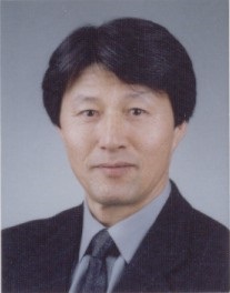
Dae-Gab Gweon |
| Professor |
| Head, Nano-Opto-Mechatronics Laboratory |
|
Division of Mechanical Engineering |
|
Korea Advanced Institute of Science and |
| Technology (KAIST) |
| South Korea |
|
Personal homepage |
| Title: Biomedical Imaging Systems for Early Detection of Disease |
|
Abstract: In this presentation, the imaging principles and applications of 4 biomedical imaging systems, confocal microscope, two-photon microscope, FLIM (fluorescence Lifetime Imaging Microscope) and spectral imaging microscope, will be introduced. The highlight of the presentation is a multimodal microscope which is the combination of the above four modalities. The diagnostic accuracy and capability can be much increased by using this multimodal microscope. For improving the accessibility of the multimodal microscope in diagnostic process, a multimodal endomicroscope was also developed in our laboratory and will be introduced in this presentation. |
|
|
 |
|
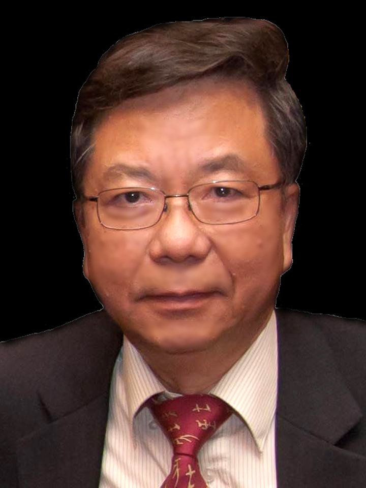
Chih-Ming Ho |
| Ben Rich-Lockheed Martin Professor |
| UCLA Distinguished Professor |
| Henry Samueli School of Engineering |
| and Applied Science |
|
University of California, Los Angeles, USA |
| Member of the US National Academy of Engineering |
| Academician of Academia Sinica |
| Personal homepage |
| Title: Manipulation of a Bio Nano Complex System for Personalized Medicine |
|
Abstract: With a newly developed feedback system control (FSC.X) technique, we can rapidly optimize the drug-dose combination for manipulating the aberrant nano components in the complex system of a specific patient. In this case, we will be able to prescribe the personalized drug for a patient, rather than just base on the disease being diagnosed. |
|
 |
|
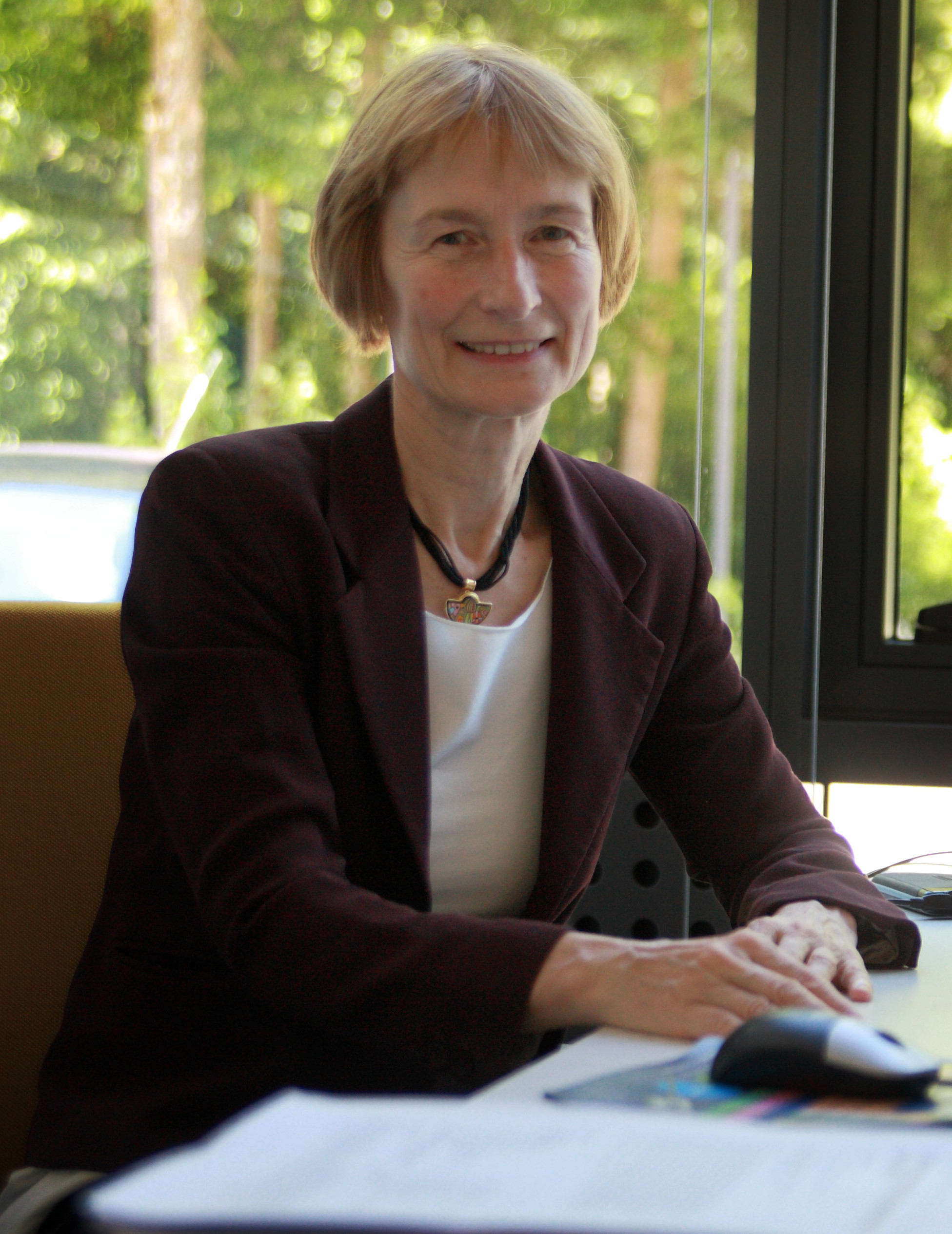
Ute Kaiser |
| Professor |
| Head, Electron Microscopy Group of Materials Science |
|
University of Ulm |
|
Germany |
|
Personal homepage |
| Title: The Atomic Structure of Low-dimensional Materials Determined from In-situ Low-voltage Aberration-corrected TEM Experiments |
|
Abstract: We report in this lecture on the atomic structure and the electronic properties of graphene and other 2D materials as well as functionalized carbon nanotubes obtained by analytical aberration-corrected transmission electron microscopy at voltages below their knock-on damage thresholds. We outline challenges, current possibilities and future prospects. |
|
|
|
 |
|
Pasi Kallio |
| Professor |
| Micro- and Nanosystems Research Lab |
|
Department of Automation Science and Engineering |
|
Tampere University of Technology, Finland |
| IEEE Finland Section Chair |
|
Personal homepage |
| Title: Micro/nanorobotic Handling and Characterization of Microscale |
| Biological Objects |
|
Abstract: This talk will discuss recent developments in micro/nanorobotic and microfluidic technologies in the handling and characterization of microscale biological objects. The talk will address challenges in stem cell research and opportunities provided by micro/nanorobotic and microfluidic technologies. It will also discuss issues in autonomous characterization of natural fibers, such as individual wood fibers. |
|
|
 |
|
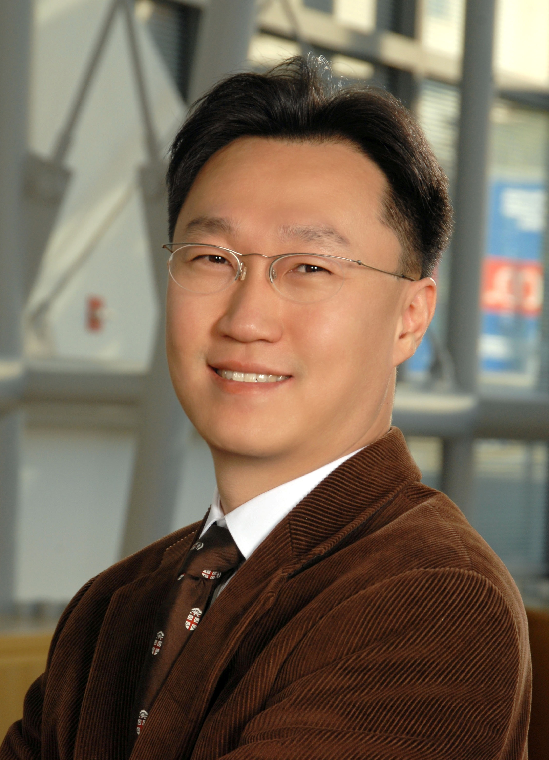
MinJun Kim |
| Professor |
| Director, Biological Actuation, Sensing and Transport |
|
Laboratory |
|
Department of Mechanical Engineering and |
| Mechanics |
|
Drexel University, Philadelphia, USA |
|
Personal homepage |
| Title: Biologically Inspired Hybrid Robotic Systems for Nanomedicine |
|
Abstract: The use of biological nanostructures in engineered systems represents a critical step toward understanding both how the biological world has evolved at the nanoscale as well as how scientists and engineers can mimic and improve on nature using modern fabrication and assembly. Two topics are treated within this talk. First, we will discuss the practical integration of biomolecular motors to actuate microscale transporters for cell manipulation. The ability to integrate multiple levels of functionality with a control hierarchy will be highlighted to show the realization of miniaturized biomedical robots. Second, this talk will be focused on a biomimetic drug delivery system with active propulsion. |
|
|
 |
|
Arkady Krasheninnikov |
| Assoc. Professor |
| Materials Physics Division, University of Helsinki |
|
Department of Applied Physics, Aalto University |
|
Helsinki, Finland |
|
Personal homepage |
| Title: Defects in Two-dimensional Materials |
|
Abstract: Two-dimensional (2D) materials like graphene, h-BN, and transition metal dichalcogenides have recently received lots of attention due to their unique properties. All these materials have defects, which naturally affect their characteristics. Moreover, defects can deliberately be introduced to tailor the properties of the system. In my talk, I will present the results of our first-principles theoretical studies of defects in 2D systems, compare them to the experimental transmission electron microscopy data, and discuss how defect and impurities can be used to engineer the electronic structure of 2D materials. |
|
|
 |
|
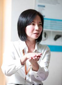
Yi-sha Ku
|
| Senior Principal Researcher |
| Project leader, Semiconductor Metrology |
| Industrial Technology Research Institute |
|
Professor |
| Institute of Photonics Technology |
| National Tsing Hua University |
|
Personal homepage |
| Title: Metrology for 3D Interconnect Processes |
|
Abstract: The 2013 ITRS expands on the new urgency for Metrology for 3D Interconnects to include wafer alignment, interface bonding, and through silicon vias (TSV). The main challenges for 3D metrology involve measuring high aspect ratio TSV, and the opaque nature of silicon wafer materials that limit conventional optical microscopy techniques. This talk presents a 3D IC metrology development status on the basis of what we have known from 3D Interconnect manufacturing process at ITRI. The main topics covered here are HAR TSV depth/profile measurement, thinned wafer thickness/bow/warpage measurement and metal film thickness measurement. |
|
|
 |
|
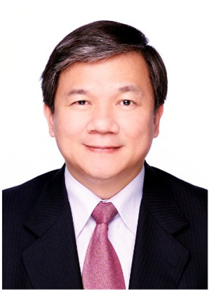
Chih-kung Lee |
| Distinguished Professor |
| Head, Wireless Nano-Bio MEMS Lab |
|
Institute of Applied Mechanics |
| Dept of Engineering Science & Ocean Engineering |
| National Taiwan University |
|
Personal homepage |
| Title: Bessel Beam Machining and Light-field Metrology |
|
Abstract: Optical based micromachining has been gaining popularity due to its flexibility and ease of use. However, traditional optical systems are affected by a diffraction limit where the focal spot size is limited by an incident wavelength and numerical aperture of the system. In order to shrink the focal spot, one approach has been to increase the numerical aperture of the lens. A lens with a larger NA can reduce the spot size but also simultaneously reduces the depth-of-focus (DOF) which increases the difficulty in system alignment. By extending the non-diffracting beam demonstrated in 1987 by Durnin, termed a Bessel beam due to its 10 to 100 times depth-of-focus when compared to that of traditional Gaussian beams, we have channeled our efforts towards adopting finite-difference time-domain (FDTD) simulation and experimentation to facilitate Bessel beam micromachining techniques. Precision metrology based on furthering the light-field techniques which can improve several traditional measurement techniques will also be examined. |
|
|
 |
|
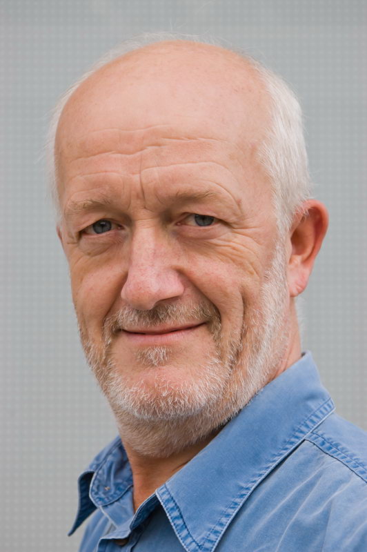
Eberhard Manske |
| Professor |
| Chair, Dept. of Precision Metrology |
|
Inst. of Process Measurement and Sensor Technology |
|
Ilmenau University of Technology, Germany |
|
Personal homepage |
| Title: Nanopositioning and Nanomeasuring Machine for Measurement, |
| Manufacturing and Manipulation on the Nanoscale |
|
Abstract: Today, nanopositioning and nanomeasuring technology provides high-precision measurement and positioning of objects across different scales, from sub-nanometres up to several centimetres. Continuing rapid progress in some key fabrication technologies structures are reaching atomic dimensions and are becoming more and more complex. The Nanopositioning and Nanomeasuring Machine, developed at the Technische Universität Ilmenau, has got a measuring range of 25 mm x 25 mm x 5 mm, 0.02 nanometer resolution. This machine is suitable not only to measure with an outstanding nanometer accuracy but also to manipulate and to fabricate on the nanoscale. |
|
|
 |
|
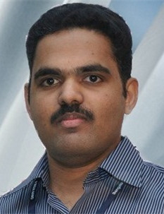
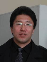
Rahul Raveendran Nair |
| Leverhulme Fellow |
| Condensed Matter Physics (Geim Lab) |
|
School of Physics and Astronomy |
|
University of Manchester, UK |
|
Personal homepage |
| Title: Properties and Application of Graphene Based Materials |
|
Abstract: In my talk, I will mainly discuss the novel properties and potential applications of various graphene based materials. Especially, I will focus on the membrane properties and applications. Graphene-based materials can have well-defined nanometer pores and can exhibit low frictional water flow inside them, making their properties of interest for filtration and separation. |
|
 |
|
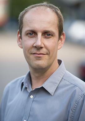
Hong-Bo Sun |
| Professor and Dean |
| College of Electronic Science and Engineering |
|
Jilin University |
|
Personal homepage |
| Title: Nano-Measurement by Transient Spectroscopies: Open the Blackbox of |
| Optoelectronic Dynamics |
|
Abstract: Low-dimensional quantum systems from conventional semiconductor nanocrystals to, nano-graphene and carbon nanodots exhibit significantly different optoelectronic properties compared with bulk materials. The origin of some unusual phenomena remains unknown, which is making an major obstacle for their broad device applications. In this talk, we will introduce typical ultrafast spectroscopic technologies such as single-photon counting, pump probe, and fluorescent upconversion transient absorption, and their applications on revealing optoelectronic and electro-optical conversion dynamics of the nano-scaled materials. |
|
 |
|
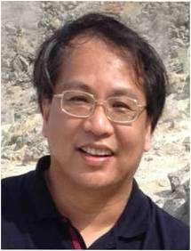
Heiko Weber |
| Professor |
| Chair, Applied Physics |
|
Institute of Condensed Matter Physics |
| University of Erlangen-Nuremberg, Germany |
|
Personal homepage |
| Title: Epitaxial Graphene on SiC: Gateless Patterning, Efficient Switches and a |
| Concept for Digital Circuits |
|
Abstract: I will present recent progress obtained with the material system epitaxial graphene on SiC (0001). In solid state electronics, functionality is related to material contrast. In that spirit, we introduce a lateral patterning of the charge density in the graphene layer by locally varying intercalation. Further, we employ the substrate SiC as a semiconductor, which can be used as semiconducting transistor channel. By combining these two material contrasts, we achieve a system which allows the design of switches with high on/off ratio as well as the definition of logical and analog circuits. A variety of functionalities is presented. |
|
 |
|
Pei-Kuen Wei |
| Associate Director and Research Fellow |
| Research Center for Applied Sciences |
| (RCAS), Academia Sinica |
|
Professor |
| Institute of Biophotonics |
| National YangMing University |
|
Personal homepage |
| Title: Fabrication and Applications of Nanostructures for Highly Efficient Light |
| Extraction |
|
Abstract: Green energy devices, such as LEDs and solar cells, suffer from low external quantum efficiency due to the limited light extraction. We designed and fabricated different shapes and dimensions of nanostructures on the devices by using nanoimprint and nanosphere lithography. For the OLEDs, the nanopillers surface with the nanomech silver anode resulted in an extraction efficiency enhancement up to 2.7 times. For the OPVs, 35% enhancement of power conversion efficiency was achieved. |
|
 |
|
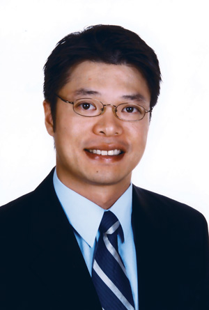
Ning Xi |
| MSU Distinguished Professor and |
| John D. Ryder Professor |
|
Dept. of Electrical and Computer Engineering |
|
Director, Robotics and Automation Laboratory |
| Michigan State University, USA |
| Personal homepage |
| Title: Non-Vector Space Control for Nano Manipulations |
|
Abstract: Nano meter positioning accuracy has been a major bottle neck in manufacturing automation in semiconductor industries. In addition, nano meter scale motion control capability will enable a direct sensing and manipulation at a molecular level, e.g. for drug discovery and disease diagnostics and treatments. In this talk a new motion control theory, i.e. non-vector space control, will be introduced. The dynamics associated with the motion control will be described in a non-vector space mathematical framework. This non-vector space dynamics model enables the development of the compressive feedback method that can overcome the major difficulties with high accuracy motion control including sensor noise and system calibration. The applications of the non-vector space motion control method will also be discussed, in particular nano manufacturing and biomedical systems. |
|
 |
|
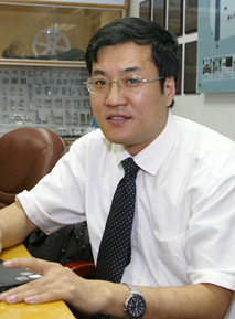
John Yeow |
| Professor |
| Canada Research Chair in Micro/Nanodevices |
|
Dept. of Systems Design Engineering |
|
University of Waterloo, Canada |
|
Personal homepage |
| Title: Row-column Addressed Capacitive Micromachined Ultrasonic |
| Imaging System |
|
Abstract: This talk will focus on the design and experimental results of a row-colum field-programmable gate array (FPGA)-based real-time ultrasound imaging system that uses 1D and 2D phased-array capacitive micromachined ultrasonic transducers (CMUTs) fabricated using a fusion bonding process. A novel row-column addressing scheme will be introduced to simplify the circuitry design as well as minimize the overall footprint of the CMUT device. |
|
 |
|
Xianmin Zhang |
| Dean and Chair Professor |
| School of Mechanical and Automotive Engineering |
|
South China University of Technology |
|
Personal homepage |
| Title: Analysis and Design of the Precision Compliant Mechanisms |
|
Abstract: Compliant mechanisms have been recognized as the most suitable mechanisms for accomplishing high-precision tasks in the field of micro/nano manipulation. This talk will present some typical analysis and design methods for compliant mechanisms. |
|
| *The list of invited speakers is based on the alphabetical order of family names. |
|
|
|

